Introduction
Serial Peripheral Interface (SPI) is a widely used synchronous communication protocol for connecting microcontrollers with peripheral devices such as sensors, displays, memory, and communication modules. It offers high-speed full-duplex communication using a master-slave architecture. STM32 microcontrollers include built-in SPI peripherals, making it easy to implement STM32 SPI communication efficiently.
This guide covers SPI fundamentals and provides an example of using SPI to communicate with an IMU sensor. By the end of this article, you will have a solid understanding of how to configure and use SPI in STM32 microcontrollers.
SPI Protocol
SPI operates using four primary signals:
MOSI (Master Out, Slave In) – Data sent from the master to the slave.
MISO (Master In, Slave Out) – Data sent from the slave to the master.
SCK (Serial Clock) – Clock signal controlled by the master.
CS/SS (Chip Select/Slave Select) – Used by the master to select the active slave.
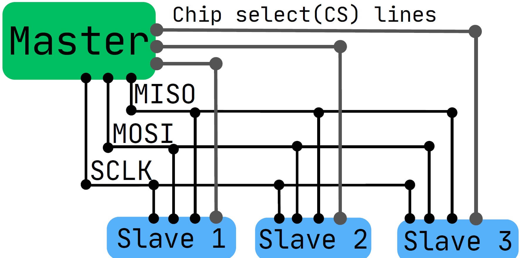
As shown in the picture below, one master can connect to multiple slave devices. All slave devices share the same MISO, MOSI, and SCLK lines, but SPI requires a separate CS line for each slave.
 SPI Illustration
If the master wants to communicate with a slave, it has to pull down the corresponding CS line, keeping the rest of the CS lines high. For example, in the illustration below, the master resets the CS line 2 low and sets CS 1&3 high to communicate with the slave in the middle.
 SPI illustration: activating slave in the middle
SPI can operate in different modes based on clock polarity (CPOL) and clock phase (CPHA).
These settings determine when data is sampled and shifted during communication. The figures below demonstrate all four possible CPOL and CPHA configurations. Usually, you must check a device's datasheet to decide which configuration suits your needs.
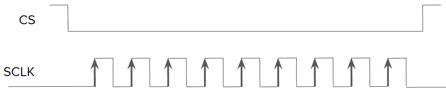 CPOL = 0 and CPHA = 0: clock is low in idle state and sampling on the leading clock edge
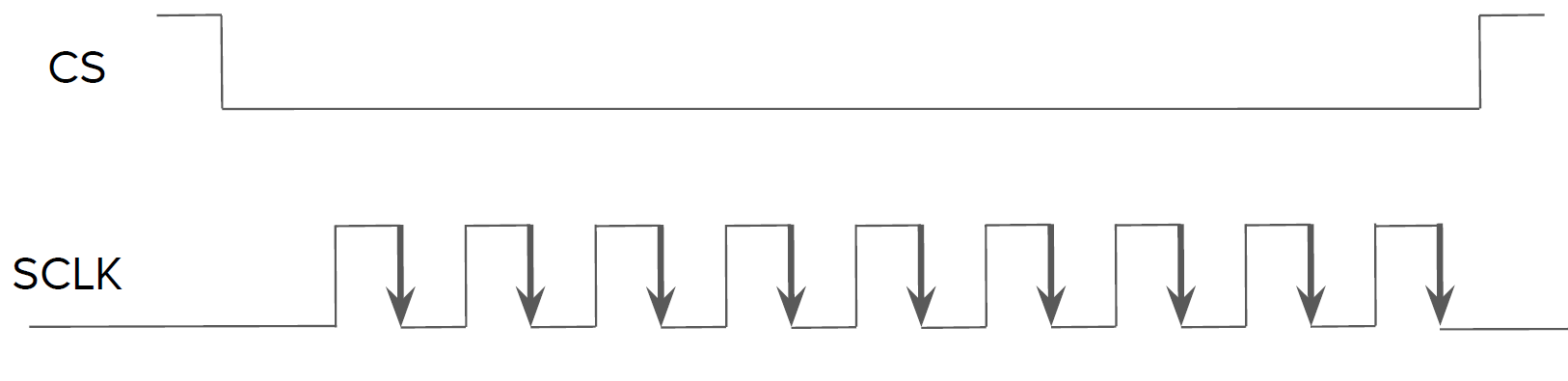 CPOL = 0 and CPHA = 1: clock is low in idle state and sampling on the second clock edge
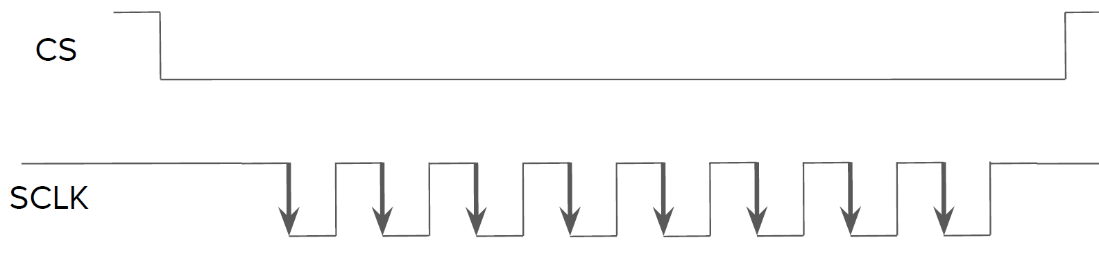
CPOL = 1 and CPHA = 0: clock is high in idle state and sampling on the
leading clock edge

STM32 SPI Receiving Data
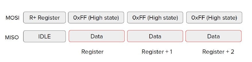
The details might vary from device to device, but receiving data through SPI generally works in the following fashion. First, transmit the register address by setting the most significant bit of the byte. Then, send a dummy 0xff byte to receive the value of the register specified. The illustration below illustrates the mechanism of reading a register.
For example, if we are willing to read register 0x57, we send ox57|0x80 ('|' is a logical OR operation) and 0xff. In return, the SPI device will return the data of 0x57.

STM32 SPI Reading Multiple Registers
Another common mechanism in SPI is reading multiple registers in a single transaction. For example, using IMU sensors requires reading several registers to obtain all axes' accleration/gyroscope values. We usually send multiple dummy 0xff to get data from consecutive registers to implement this mechanism. For example, if we send 0x57|0x80 and three 0xff, we receive data from 0x57, 0x58, and 0x59.
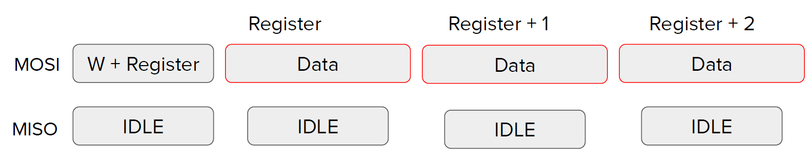
SPI Writing to Registers
Writing to the registers works in the same fashion as the reading mechanism. First, the master has to send the register address to write the data, but setting the MSB is needed. The multiple bytes are followed, which will be written to consecutive registers. For example, if the master sends ox57 and three bytes, this data will be written to registers 0x57, 0x58, and ox59.
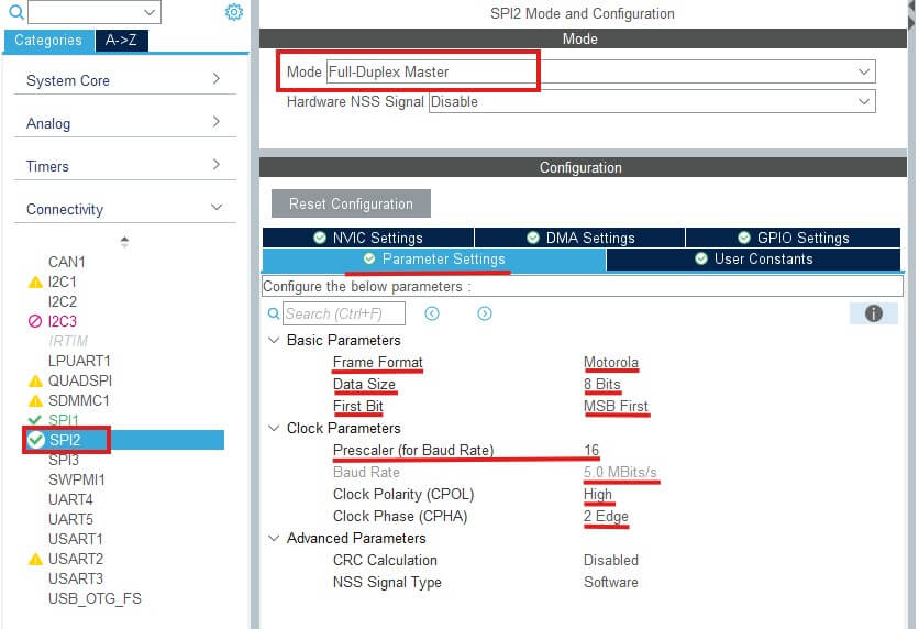
STM32 STM32CubeMx Configuration
Finally, we focus on the practical aspect: configuring SPI in STM32CuebMx. After creating a project, choose the SPI within the Connectivity category. We need to define the frame format and other configurations in the Parameter settings. Fame Format is Motorola (I have never encountered SPI with a different frame format), and Data Size is 8 bits. Also, the first bit is MSB in most cases, but you can also check the device's datasheet to be sure. Then, we set the prescaler to define the Baud rate. Usually, you can find the maximum allowable data rate within the datasheet. Set a correct baud rate not to exceed this value. Finally, we use the datasheet to set the correct CPOL and CPHA polarities.
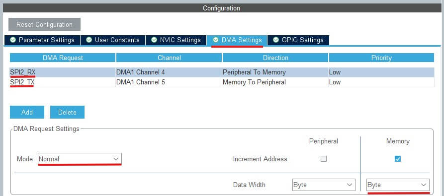
In addition, we can enable DMA for both data transmission and reception. For that, open the DMA settings and add DMA RX and TX. The default configurations should be sufficient.
Enable Interrupts for the future use. 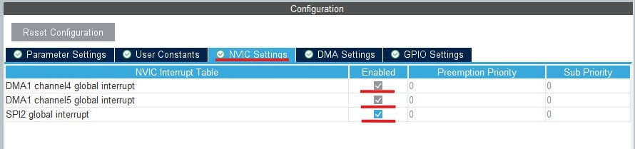
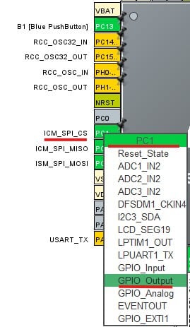
Finally, do not forget to configure one of the pins as GPIO OUT to use it as Chip Select (CS) Pin. After all these configurations, save the file to generate the code
STM32 SPI Transmit/Receive using Polling Mode
The list below presents STM32 SPI Functions in Polling Mode:
- HAL_SPI_Transmit()
- HAL_SPI_Receive()
- HAL_SPI_TransmitReceive()
Polling/blocking mode means these functions block the program, so the program must receive/transmit data before moving to the next step.
SPI Receive Data
Finally, we can implement a function to read a register of the IMU Sensor. As we discussed, we need to transfer the register setting the MSB, and the IMU sensor should return the register data. Also, we should not forget to reset the CS pin to activate the SPI device.
void mpu9250_read_reg(uint8_t reg, uint8_t *data, uint8_t len)
{
   uint8_t temp_data = 0x80|reg;
   HAL_GPIO_WritePin(MPU_IMU_CS_GPIO_Port, MPU_IMU_CS_Pin, GPIO_PIN_RESET);
   HAL_SPI_Transmit(&MPU_IMU_SPI, &temp_data, 1, 100);
   HAL_SPI_Receive(&MPU_IMU_SPI, data, len, 100);
   HAL_GPIO_WritePin(MPU_IMU_CS_GPIO_Port, MPU_IMU_CS_Pin, GPIO_PIN_SET);
}
SPI Transmit Data
Similarly, we can define a function to transmit data. In this case, we transmit the register address followed by data.
void mpu9250_write_reg(uint8_t reg, uint8_t data)
{
HAL_GPIO_WritePin(MPU_IMU_CS_GPIO_Port, MPU_IMU_CS_Pin, GPIO_PIN_RESET);
HAL_SPI_Transmit(&MPU_IMU_SPI, ®, 1, 100);
HAL_SPI_Transmit(&MPU_IMU_SPI, &data, 1, 100);
HAL_GPIO_WritePin(MPU_IMU_CS_GPIO_Port, MPU_IMU_CS_Pin, GPIO_PIN_SET);
}Example of reading the MPU9250 IMU data
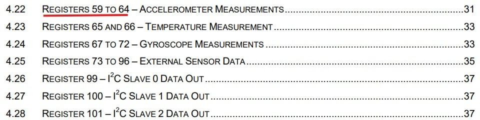
Finally, let me show how we can read the accelerometer data. If you check the register map of the MPU9250 IMU sensor, Registers between 59 and 64 hold the acceleration data. In other words, 2 bytes for each axis.

We can read the acceleration data using the code snippet within the main function below. Starting from register 59, we obtain 6 bytes, and it is essential to combine consecutive bytes to obtain 16-bit signed acceleration data.
int16_t accel_data_x, accel_data_y, accel_data_z;
uint8_t imu_data[6]  // to read raw register values
while(1)
{
   void mpu9250_read_reg(59, imu_data, 6);
   accel_data_x = ((int16_t)imu_data[0]<<8) + imu_data[1]
   accel_data_y = ((int16_t)imu_data[2]<<8) + imu_data[3]
   accel_data_z = ((int16_t)imu_data[4]<<8) + imu_data[5]
   HAL_Delay(1000);
}
STM32 SPI Video Tutorials
Other Relevant Articles